

")
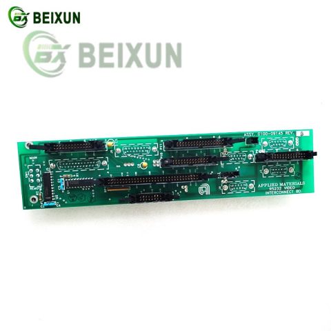
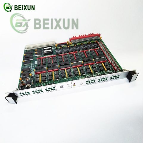
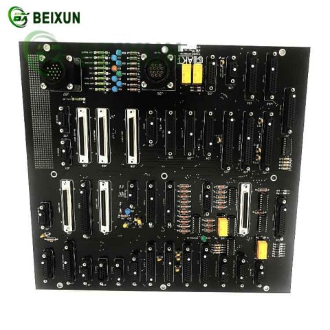
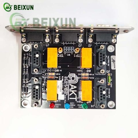
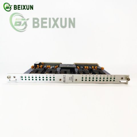
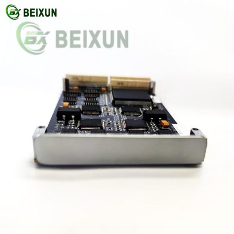
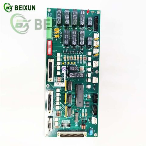
The AMAT 0100-09123 Wafer Sensor Board is a specialized PCBA (Printed Circuit Board Assembly) designed for semiconductor wafer handling and process monitoring in precision manufacturing environments.
Below are its key functions and applications:
1. Key Functions:
Wafer Position Detection:
Monitors wafer alignment and positioning in semiconductor tools (e.g., lithography, deposition systems) to ensure precision processing.
Uses high-sensitivity sensors to detect wafer presence, tilt, or misalignment.
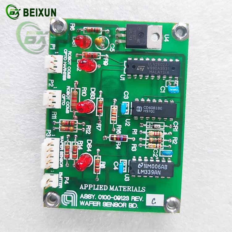
Signal Processing & Interface:
Converts analog sensor signals (e.g., capacitive, optical) into digital data for real-time control via industrial communication protocols (e.g., RS-485, Modbus).
Integrates with PLC/DCS systems for automation feedback loops.
Industrial Compatibility:
Designed to operate in high-EMI environments with stable performance in cleanroom/wafer fab settings.
2. Applications:
Semiconductor Manufacturing: Used in wafer scanning, edge detection, and load-lock chambers to prevent wafer damage.
Process Control: Deployed in chemical vapor deposition (CVD) and etching tools for real-time wafer tracking.
There are no reviews yet.